Quality control of wafers
Contact angle and surface free energy as parameters for the structure of homogenous, functional wafer layers
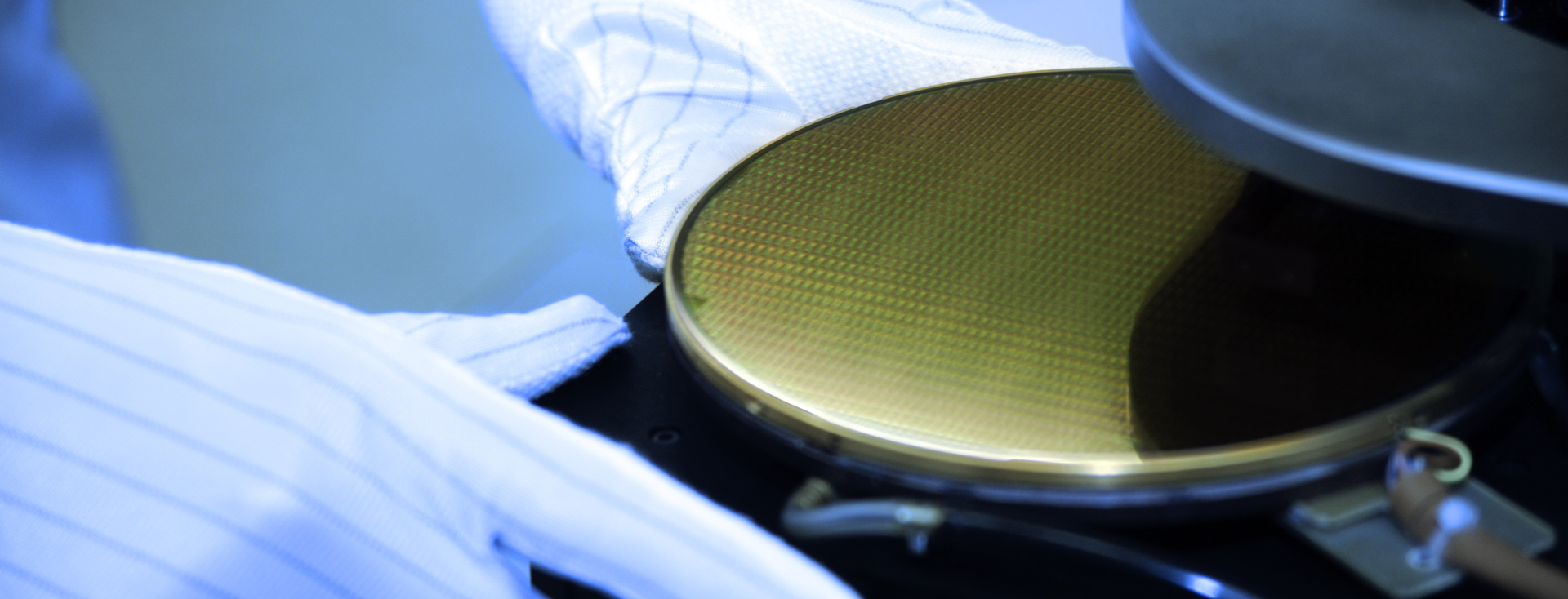
The demands on quality assurance in the production of semiconductors are very high. The wafers for manufacturing the chips have an extremely homogenous surface, and any faults in this surface give rise to high costs. The same applies to the steps involved in processing the wafer surface, such as the application of bonding agents and photo varnish as well as the complete removal of the photo varnish after exposure and etching. The homogeneity of the wafer surfaces and the success of the processing steps can be investigated with the help of contact angle measurements.
Contact angle measurements for investigating the surface homogeneity
The nature of the material must not be changed when checking the quality of the wafer surface. Contact angle measurements with ultra-pure water using our drop shape analysis instruments enable wafers to be tested non-destructively. The contact angle, as a measure of the wettability, responds sensitively to the smallest changes in the surface structure.
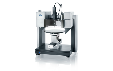
In fully automatic measuring mode with our contact angle measuring instruments, the sample can be positioned using a special wafer table, the drop is dispensed and its shape analyzed. A fully automatic series of measurements can be carried out based on previously defined measuring positions ("mapping"). The position-dependent contact angle which is displayed describes the homogeneity of the sample or represents differences between different areas, for example exposed and unexposed regions of a photo varnish layer.
Characterization of the surface treatment for direct bonding
Direct bonding describes a process in which wafer surfaces are bonded to one another in order to build up multilayer structures, for example for high-frequency technology. The necessarily strong bonding forces can be produced at high temperatures above 900 °C which, however, are clearly too high for wafers with functional layers. By appropriately pre-treating the wafers, for example using oxygen plasma, good adhesion is also achieved at low temperatures.
In order to measure the quality of the pre-treatment, the surface energy of the wafer is determined based on the contact angle with several liquids. The increase in surface energy, and in particular its polar fraction, is an indication of the surface activation and therefore successful bonding.


